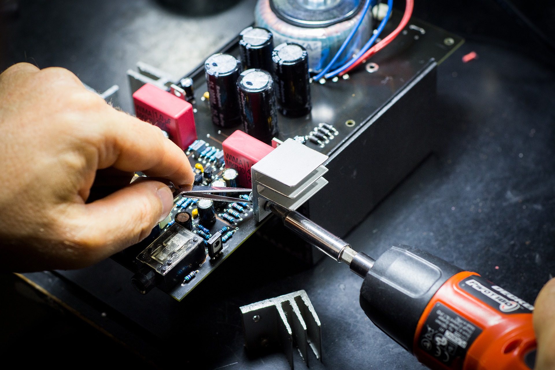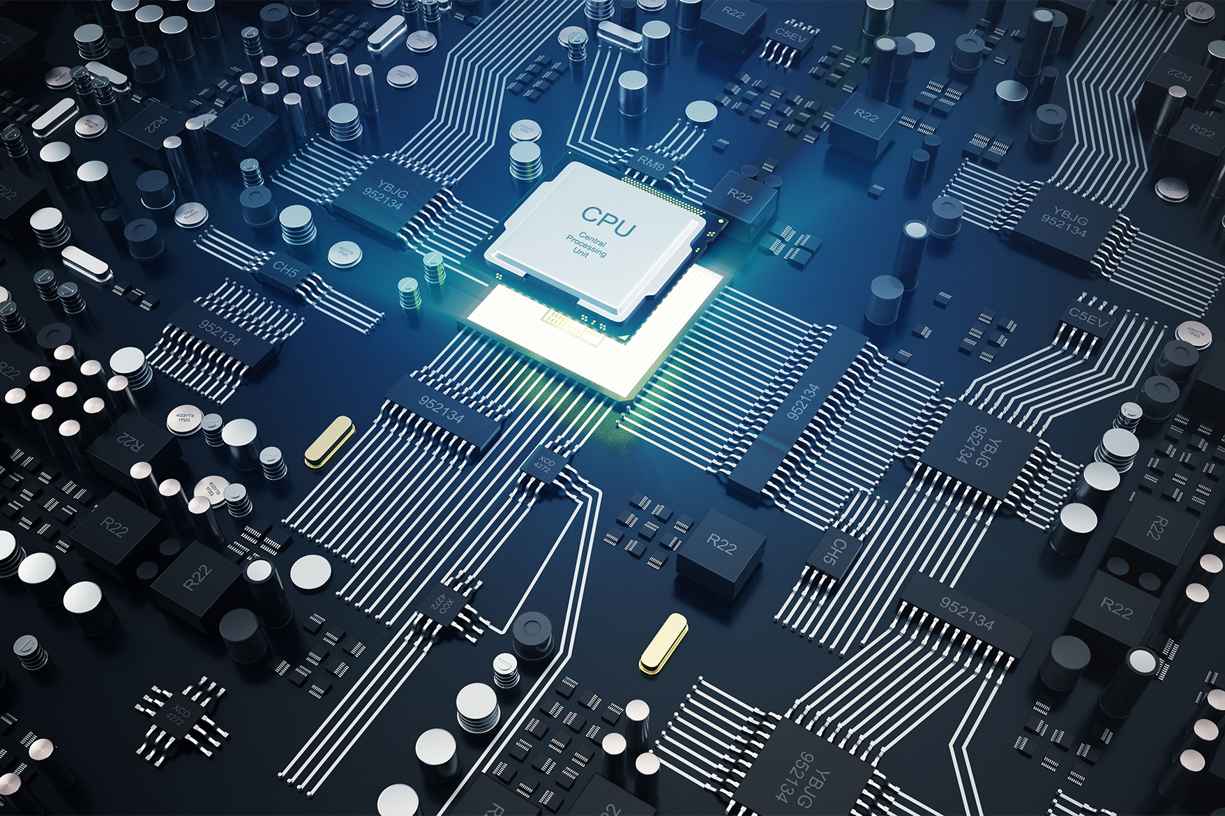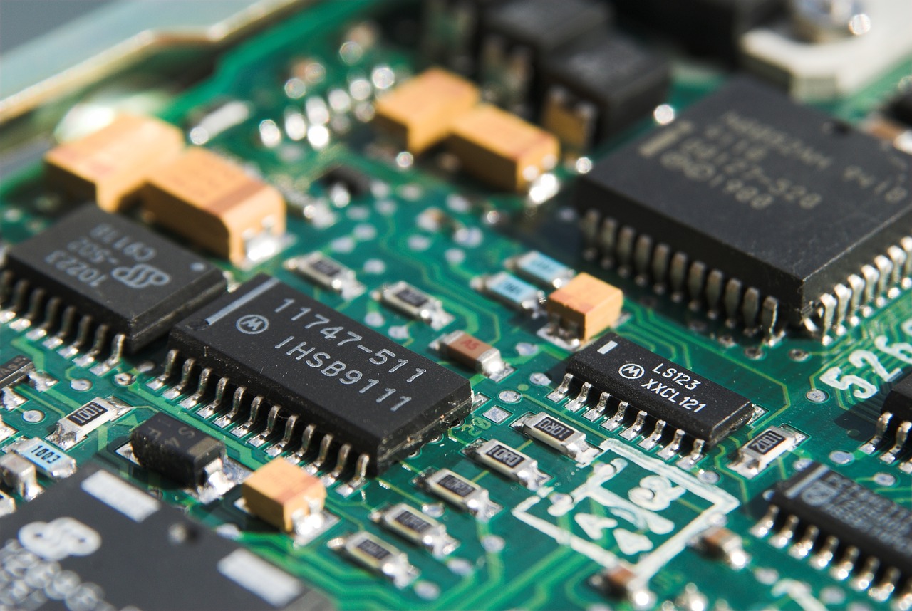
It does not matter if you are an experienced design engineer or a complete novice when it comes to an industrial PCB design. What matters is that for every piece of electronic appliance or industrial mechanical device, there is an printed circuit board (PCB) that plays an important role. These green boards provide the physical platform for the design of a complete electronics system with circuits and components together.
It is said correctly that the success or failure of any product’s function largely depends on the PCB layout product design and development. While PCB manufacturing (PCBM) and the PCB assembly (PCBA) are two different processes with their own unique requirements, they both have PCB design as a common factor.
The astounding level of technical advancements in embedded and semiconductor integration is resulting in shrinking the PCB designs. PCB layout and design services must consider the complexity and expectations of these designs that is reaching new heights.
In this blog, we outline the top ten tips or guidelines for industrial PCB product design and development.
1.Identifying the project need
The customer’s requirements dictates every embedded hardware design. This essentially involves thorough analysis of your project, budget, and requirements. Translating these requirements into an electronic form uses the technical skills and experience of an electronic design engineer. What is the type of your product, what is its operating environment; what are the powering options, communication mechanisms or the specifications/regulations does it comply? These are some questions that come to the PCB design engineers. Having these answers will help in identifying the best possible layout, initial schematic of the PCB, as well as the BOM and other details of your final PCB design.
2.Schematics:
The schematic diagram is the blueprint for PCB manufacturers and assemblers during the production processes. It is a diagrammatic representation of the electronic component symbols and the interconnections between them. Once all the design choices for the various components is finalised, this acts as baseline for developing the schematic design. Preliminary review and analysis is then performed to check for potential problems and then the corrected version is fed to the PCB design software, which can run simulations to ensure the correct functionality of the PCB. Some of the popular software are Eagle, KiCAD, Altium Designer and OrCAD.
3.Bill of Materials:
A bill of materials (BOM) is generated simultaneously along with the schematic’s creation. This is very handy as it lists out each components quantity, numerical values (like ohms, farads, voltage etc.), component part number, the reference designators and PCB footprint for each component. It defines how each component in the circuits is identified and located; the circuit element numbers used for purchasing and substitution, its size with respect to the PCB size etc. An updated BOM will save many complications in the later PCB design stage process.
4.Component placement:
Placing each component in its designated spot on a circuit board is the most critical part of designing. A wrong placement can cause various thermal, electrical noise and power variations in the circuits leading to malfunction of the PCB board and product failure. The design schematic generated earlier is used to determining the correct spot. The most common order of component placement followed by the designers are:
• Connectors
• Power circuits
• Sensitive and precision circuits
• Critical circuit components
• All other elements
The designer then verifies and reviews the initial component placement step and adjusts to facilitate routing and optimize performance. It is adjusted based on the cost and size factor also. Due considerations are given to
• PCB component placement with ground separation, power and isolation between high frequency components
• Place components with the same orientation for assembly easiness
• Print the layout to see if components’ sizes match to avoid any assembly and mechanical issue
At this point based on the size and cost, the placement and package sizes are often reconsidered and changes are made.
5.Thermal Management:
One of the most frequent design issue is thermal management of the PCBs. When heat dissipation is not considered, it leads to poor circuit performance or even a damaged board. Following are some tips to achieve high performance keeping the heating issues in mind:
• Place heat sensitive components (like thermocouples or electrolytic capacitors) away from heat generating components (like diodes, inductors, and resistors)
• Use PCB as heatsinks by using more layers of solid ground or power planes connected directly to heat sources with multiple vias
• Thermal vias dissipate heat from one side of the PCB to another. Having larger and multiple thermal vias lowers the operating temperature of components and contribute to higher reliability.
6.Wiring Considerations:
PCB wiring design is often a complicated process involving the power cord design, ground wire design and other wiring considerations. It is grouped into single wiring, double-sided wiring and multilayer wiring. It is good practice to follow some of the tips:
• Exchange wiring directions between layers. For multiple layers, alternate between directions
• Keep wiring and the distance between the wires uniform and equal
• Allow small loops in loop back wiring
• Ensure smooth soldering of the wiring
• Printed wiring corners should be rounded corners when used for circuit wire for dense or high frequency circuits
7.Mechanical Constraints:
Consider the mechanical constraints in advance before starting the placement and review during the embedded hardware design. There board materials used to create the PCB, the number of layers each PCB will have, the copper traces used to complete the connections, component selection based on availability, numbers, package type, cost and other determining factors. The PCB shape, size and board area are constrained by the PCB hosting cabinet used by the appliance or equipment.
8.Power Constraints:
Any huge current spikes or large voltage changes can interfere with the low voltage and current control circuits. A good power design guideline includes adequate separation, placement and coupling into its schematics.
In the PCB design, it’s recommended to use common rails for each supply, avoid longer power loop while routing and have solid and wide traces. Having separate power and ground planes internal to your PCB while also being symmetrical and centred will help to prevent your board from bending. You can place a small impedance path to reduce the risk of any power circuit interference and to help protect your control signals. The can be followed to keep your digital and analog ground separate.
9.Routing details:
A differential signaling is the process of using not just one, but two traces to transmit a signal on your board. They are (ideally) equal in magnitude and opposite in polarity, thus in the ideal case there is no net return current flow through ground.
There are many reasons for using a differential signaling like reducing the EMI, having precise timing to determine the current logic state a differential pair and separating the power systems.
To achieve the above benefits, it is recommended that you always route the differential signal traces in parallel, keep them as shortly and directly as possible between components. Also, maintain equal length and width of the traces while keeping the spacing constant between the trace pairs.
10.Perform Quality Checks:
One of the good practice of PCB layout and design services is to conduct a DFM and DFT checklist review before signing off your PCB designs for generating the Gerber files. The Gerber format is an open 2D binary vector image file format, which is used universally by the PCB design software. It describes the PCB images and are necessary to manufacture and assembly the final PCB boards. Some of the checklist involves verification of the component placements, routing paths, pre-scan for the thermal integrity and signal integrity among others.
Find an Assembly Service for Your PCB Design
Industrial PCB design can be a formidable task but by following the above basic techniques and best practices, it can lay the foundation for your success. Our expert product design engineering services can guide you with your next PCB design project with cost-effective services and assured quality standards.
Contact us today to learn more about the industrial product design engineering services, the PCB design rules and assembly processes.